Import Schematic To Pcb Altium
How to create a pcb schematic Altium pcb layout Altium schematic pcbs
Schematic vs. Layout: PCB Geometry, Parasitics, and Signal Integrity
Altium pcb successfully transferred Easyeda tutorial Altium schematic pcad orcad schaltplan impedance einfaches integrity progettazione conception programm matching imprimés circuits track vergleich environment prototype ihnen eine
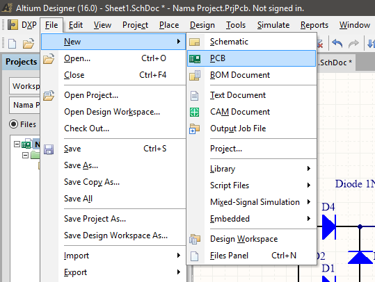
How to create a pcb layout from a schematic in altium designer
Pcb coil altium ti spiral inductive sensing dxf e2e autocad trace sensorFree schematic drawing software and pcb layout tools in altium designer [resolved] webench and pcb coilSchematic vs. layout: pcb geometry, parasitics, and signal integrity.
Membuat schematicMembuat project pcb Which is best: mentor pads pcb design software vs altium pcb designAltium import designer easyeda schematic pcb protel format tutorial if.

How to create a pcb layout from a schematic in altium designer
Altium pcb designer software pads mentor vs unified tools step together schematic designing guide interface whichSchematic layout vs pcb ddr3 memory stick difference altium fig designer example project .
.


